Set PCB antenna RF
Introduction
Printed circuit board (PCB) antennas are widely used in various wireless communication applications due to their compact size, cost-effectiveness, and good electrical performance. However, designing an efficient and reliable PCB antenna requires careful consideration of various factors, including the operating frequency, form factor, desired radiation pattern, and materials used. In this article, we will discuss how to tune a PCB antenna for optimal RF performance.
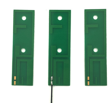
Antenna Design Considerations
Before we dive into the tuning process, let's review some key antenna design considerations:
1. Operating Frequency: The antenna's operating frequency must match the frequency band of the wireless system for which it is designed.
2. Form Factor: The antenna's physical size and shape should be optimized for the application, taking into account space constraints, aesthetic requirements, and performance objectives.
3. Radiation Pattern: The antenna's radiation pattern, or the way in which it emits radio waves, can be controlled by adjusting its shape and orientation.
4. Materials: The choice of materials for the antenna substrate and conductive elements can affect the antenna's performance, such as gain, efficiency, and impedance matching.
Tuning Process
Once the antenna design has been finalized, it is important to verify its RF performance and make any necessary adjustments to optimize its performance. The following steps outline the tuning process:
1. Determine Ideal Resonance Frequency: The first step is to determine the antenna's ideal resonance frequency, or the frequency at which it transmits and receives signals with maximum efficiency. This frequency can be calculated using standard formulas, such as the quarter-wavelength formula for a monopole antenna or the half-wavelength formula for a dipole antenna.
2. Measure Antenna Impedance: The next step is to measure the antenna's impedance, or how the antenna interacts with the impedance of the transmission line or matching network that connects it to the RF circuitry. A vector network analyzer (VNA) or antenna analyzer can be used to measure the antenna's reflection coefficient, or S11 parameter, and impedance matching can be performed using lumped or distributed components.
3. Adjust Antenna Parameters: Based on the impedance measurement, adjustments can be made to the antenna's physical dimensions, such as the length or width of the radiating element or the spacing between elements, to fine-tune the impedance matching. This can be done by adding or removing copper or dielectric material from the antenna structure or by changing the feed point location.
4. Measure Radiation Pattern: Finally, the antenna's radiation pattern can be measured using an anechoic chamber or other testing facility. This step confirms that the antenna's radiation characteristics match the desired pattern for the application.
Conclusion
Tuning a PCB antenna for optimal RF performance requires careful consideration of several factors, including operating frequency, form factor, radiation pattern, and materials used. By following the tuning process outlined above and making adjustments to the antenna's physical parameters and impedance matching, the antenna's efficiency, gain, and overall performance can be optimized. With a well-tuned PCB antenna, wireless communication systems can achieve reliable and high-quality performance.
